

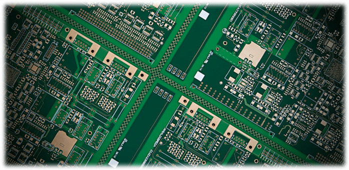
When you look at a modern electronic device—be it a smartphone, wearable, or high-performance computing system—it’s easy to admire the sleek interface and impressive functionality. But what you don’t see is the incredibly complex engineering underneath. You’re actually relying on a marvel of miniaturized electrical architecture: the HDI Printed Circuit Board, or HDI PCB. As a professional or enthusiast in the electronics industry, understanding the intricacies of HDI PCB design can give you a significant edge, especially when working with an experienced manufacturer like Pcb-Togo Electronic, Inc.
What is an HDI PCB?
An HDI Printed Circuit Board (High-Density Interconnect PCB) is a type of PCB that incorporates a higher wiring density per unit area than traditional circuit boards. This is accomplished through finer lines and spaces, smaller vias, and higher connection pad density. If you’re designing for advanced functionality in a compact space, HDI technology is not a luxury—it’s a necessity.
HDI PCBs are commonly used in smartphones, tablets, GPS units, automotive electronics, and other applications where space and weight are at a premium. But behind the scenes of this tiny powerhouse lies a web of invisible complexity.
Why HDI PCB Design is So Challenging
You might think that designing an HDI PCB is just about making things smaller. In reality, it’s much more than that. When you scale down, the design challenges scale up. Here are some of the critical complexities you need to navigate:
1. Signal Integrity and High-Speed Design
As data speeds increase, maintaining signal integrity becomes paramount. HDI boards often support high-frequency signals, which means even slight design flaws can lead to performance issues. You need to consider impedance control, cross-talk minimization, and return path continuity in your layout. Each trace must be meticulously planned—there’s little room for error.
2. Via Structures and Layer Stacking
HDI PCBs rely heavily on microvias, blind vias, and buried vias. These different types of vias allow interconnection between layers without taking up excessive space. However, their use introduces complexity in fabrication and assembly. You must carefully plan the layer stack-up, considering how each via will be drilled, plated, and interconnected. Poor via design can lead to failures during reflow or in the field.
3. Thermal Management
With components packed tightly together, managing heat becomes a significant concern. You have to design with thermal vias, heat sinks, and careful component placement. An overlooked thermal issue can compromise the reliability of your entire product.
4. Manufacturing Constraints
Not all manufacturers can handle the demands of HDI PCB fabrication. You need a trusted partner like Pcb-Togo Electronic, Inc, which specializes in high-precision manufacturing. They understand the exacting standards required, from laser drilling microvias to stacking multiple layers with minimal deviation.
The Design Process: A Strategic Balance
When you embark on an HDI PCB project, you’re not just working with lines and layers—you’re managing a strategic balance between performance, cost, and manufacturability.
Design for Manufacturability (DFM)
It’s vital to collaborate with your manufacturing partner from the beginning. Companies like Pcb-Togo Electronic, Inc offer design reviews and DFM analysis, ensuring your layout is both functional and producible. This partnership saves you time, reduces rework, and minimizes the risk of design failure.
Component Placement and Routing
With less real estate, you have to make every millimeter count. Your component placement needs to follow logical signal paths while considering heat dissipation and mechanical constraints. Routing becomes a game of 3D chess, requiring you to think in layers and anticipate interactions across the entire board.
Cost Optimization
Advanced technologies like stacked vias and sequential lamination can drive up costs quickly. But with the right strategy, you can optimize your design without sacrificing performance. For example, using via-in-pad technology can reduce the number of layers required while improving signal performance.
Tools and Techniques You Should Use
If you’re designing HDI boards, your toolkit needs to be up to the task. Here are a few industry best practices you should follow:
- Use advanced EDA software with HDI capabilities such as Altium Designer or Cadence Allegro.
- Simulate signal integrity before fabrication to catch potential problems early.
- Employ design rules tailored for HDI, including tighter spacing, finer trace widths, and specialized via parameters.
- Work closely with your fabrication partner to understand their capabilities and limitations.
Pcb-Togo Electronic, Inc: Your HDI PCB Partner
Navigating HDI design complexity requires more than just good software—it requires a knowledgeable partner who’s been through it before. Pcb-Togo Electronic, Inc has the experience and infrastructure needed to deliver HDI PCBs that meet your exact specifications. From prototyping to full-scale production, they provide end-to-end support tailored to your project’s needs.
Their team is skilled in advanced techniques like laser drilling, sequential lamination, and via filling, ensuring every detail of your design is realized accurately. More importantly, they’re committed to quality assurance at every step, using rigorous testing and inspection methods to guarantee performance and reliability.
Whether you’re building a medical device, an automotive controller, or the next breakthrough in mobile technology, Pcb-Togo Electronic, Inc can help you bring your ideas to life. If you’re ready to start your next HDI PCB project, don’t hesitate—contact us today.
Conclusion:
The invisible complexity of HDI PCB design is what enables the visible innovation in modern electronics. As someone who creates or engineers these devices, you must go beyond surface-level understanding. Dive into the details—materials, vias, thermal paths, signal flows. Each decision you make affects not just functionality, but manufacturability and reliability.
By choosing a trusted partner like Pcb-Togo Electronic, Inc, you gain not just a manufacturer, but a collaborator who understands your goals and the technical intricacies that make them possible. So when you’re designing your next high-performance, miniaturized marvel, remember: the real magic happens in the layers you don’t see.
